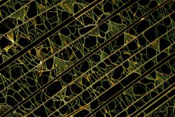
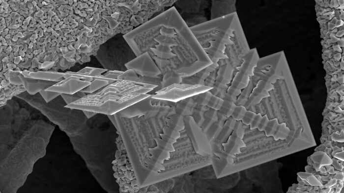
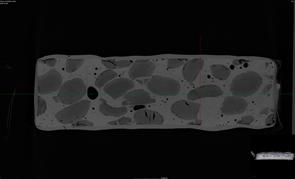
March 2026
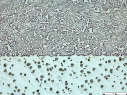
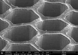
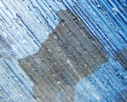
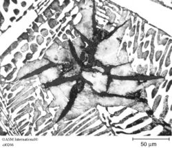
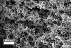
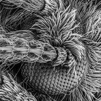
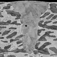
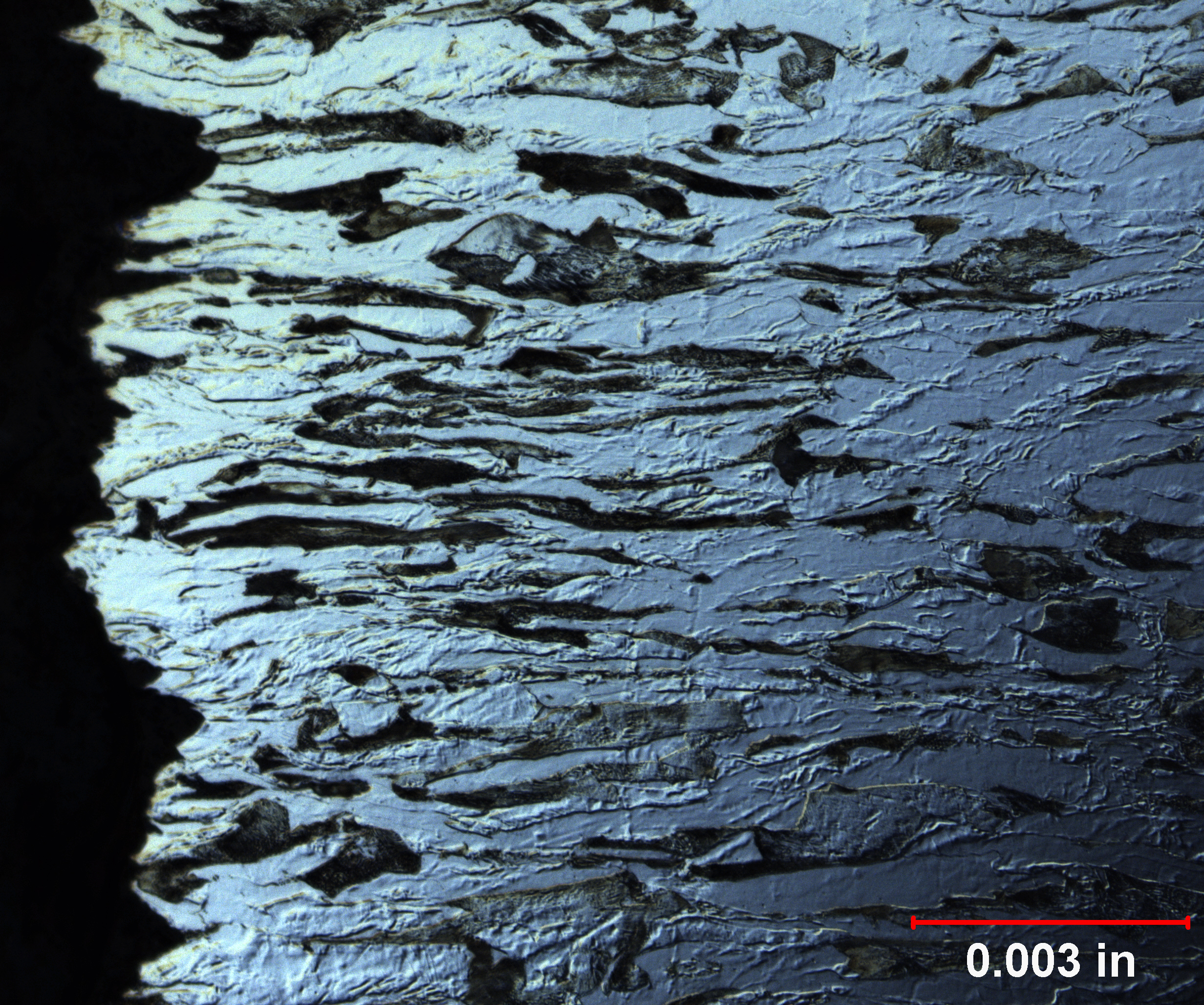
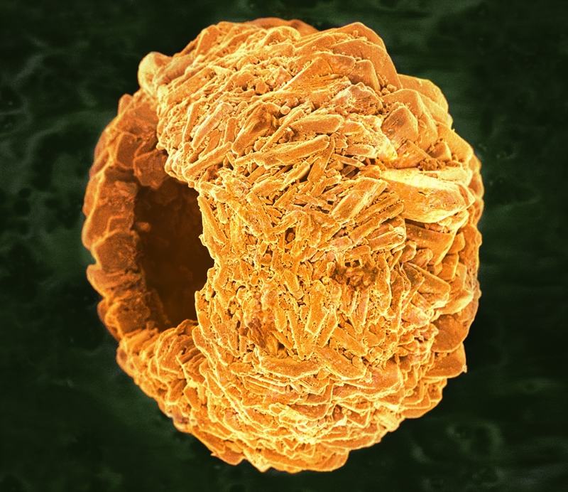
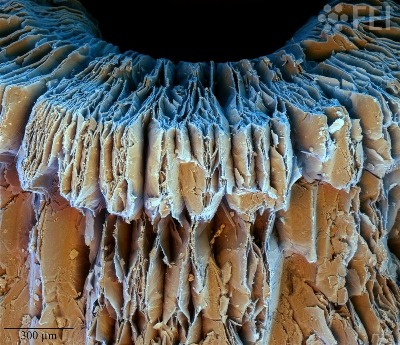
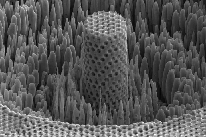
This micrograph, though it resembles a popular flavor of ice cream, is actually an atmosphere brazed tungsten carbide coating on gray cast iron. The image appears in “Additive Brazing for New Part Production, Remanufacturing, and Wear Protection,” which is the lead article and graces the cover of the March 2026 issue of Advanced Materials & Processes magazine. The image and article are courtesy of Euromat GmbH.
See image on AM&P cover
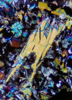
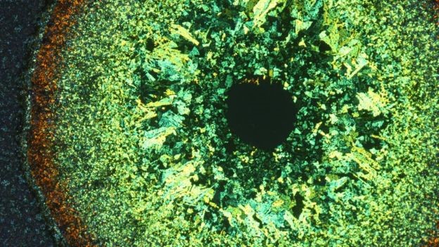
February 2026
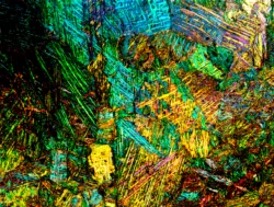
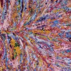
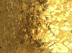
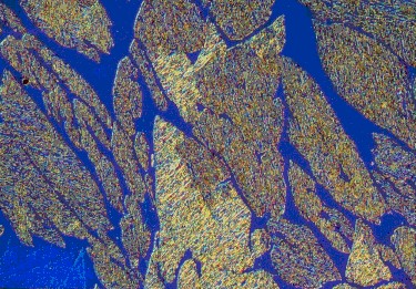
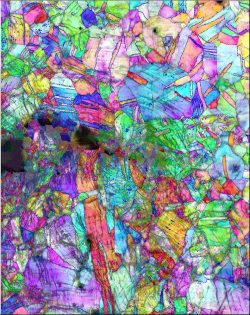
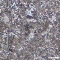
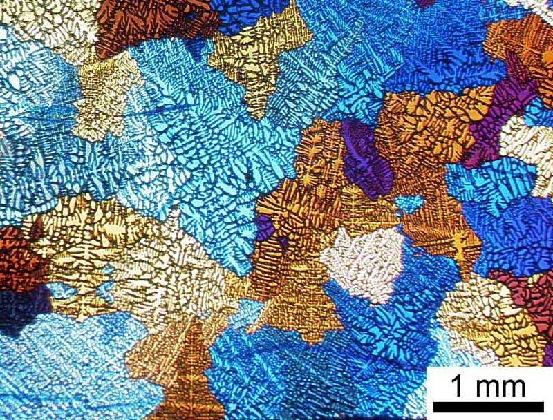
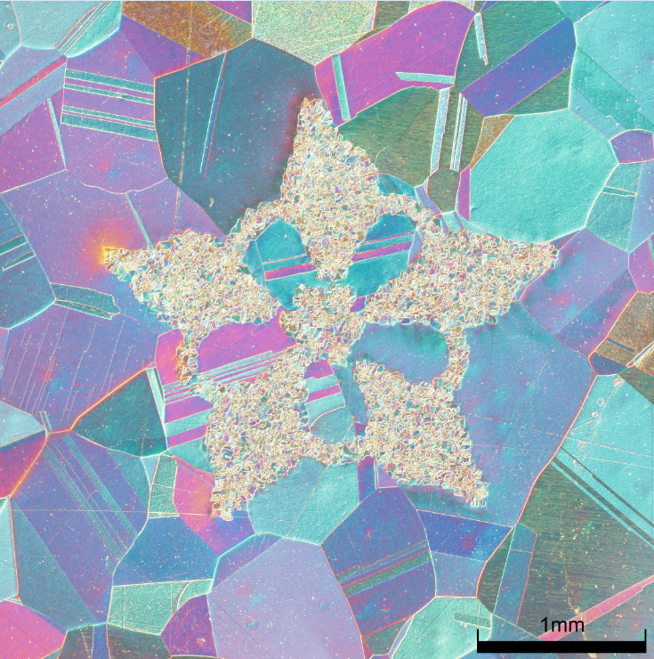
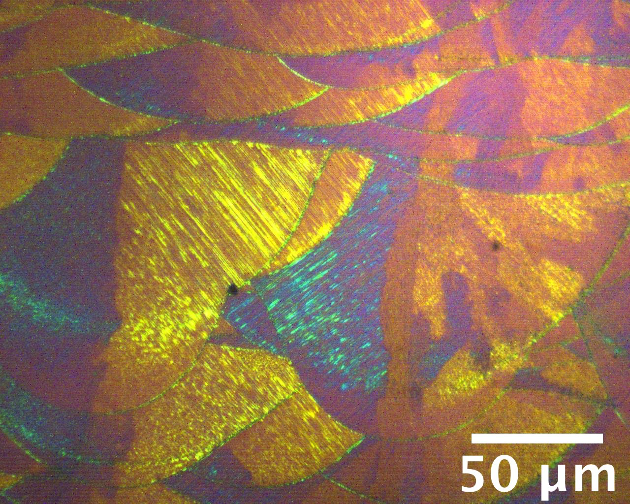
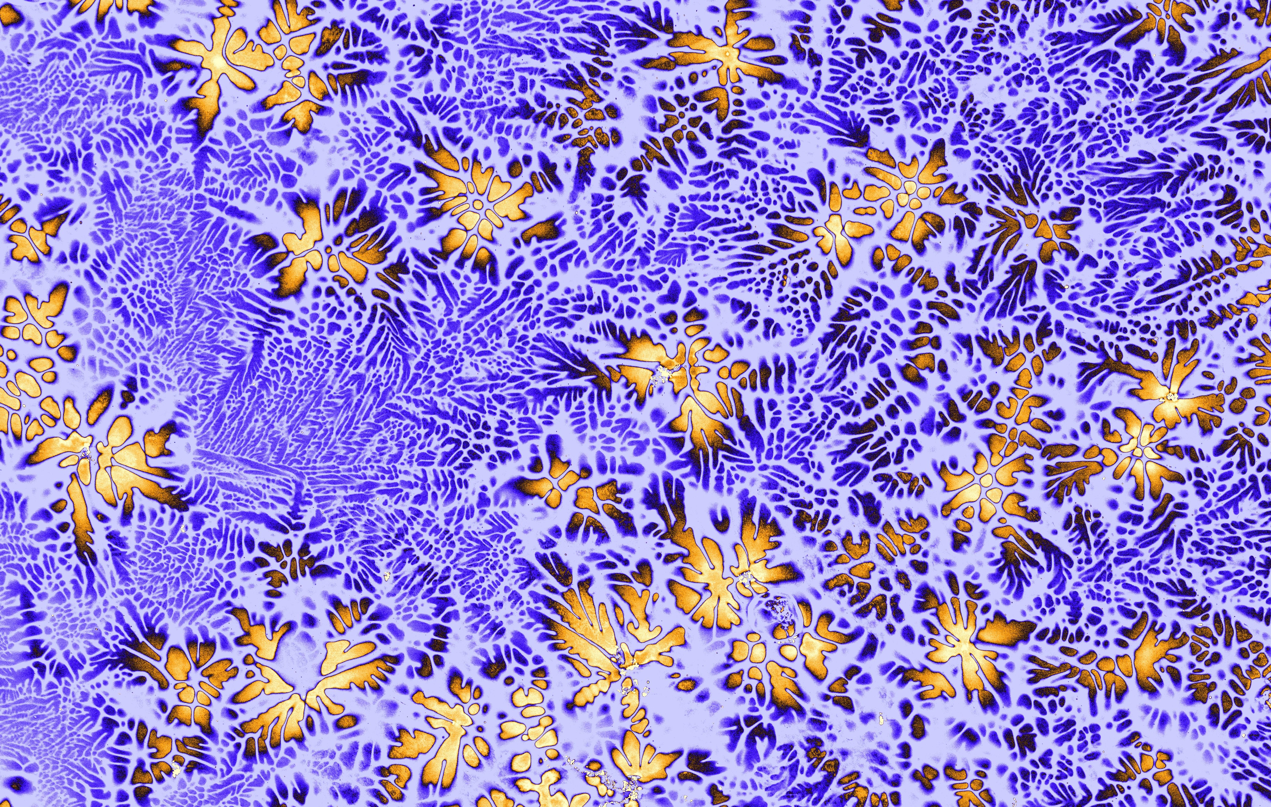
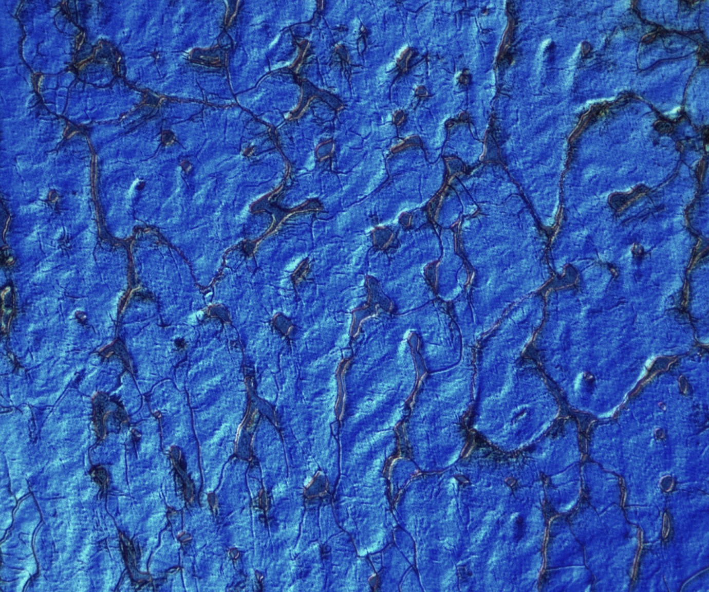
Metallography, Microstructure, and Analysis (MMA) will feature new cover art in 2026! The image shown, which was selected as the new cover art, is a Ni-Mn-Ga Shape memory alloy. The photo was captured using a 5x/0.13 objective with polarized light, with an AxioCam 503C camera. The colors visible in the sample are also interference colors and depend on the crystalline structure of the sample and the orientation of this structure vs. the polarizing filters in the microscope. The image is courtesy of José Manuel Martínez López, Química Tech, México. It originally appeared in Metallography, Microstructure, and Analysis in the April 2025 issue as a MicroArt submission. Metallogr. Microstruct. Anal. 14(2), 454 (2025).
IMS members receive free online access to Metallography, Microstructure, and Analysis.
January 2026

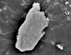
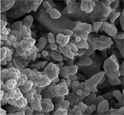
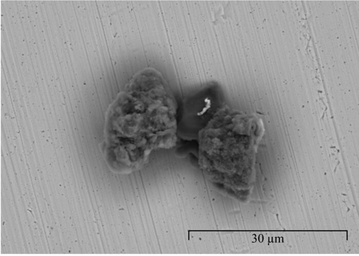
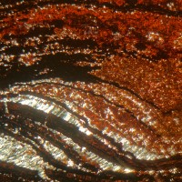
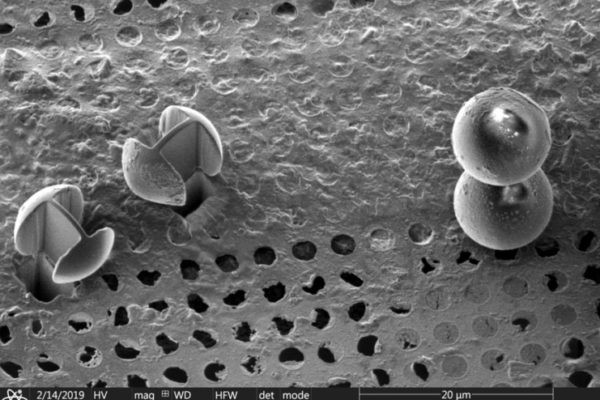
This image is the result of an SEM-EDS chemical analysis of a battery electrode precursor powder. It was captured using Gemini 460 and Oxford Instruments Ultim Extreme windowless EDS detector. It was featured as the November image in the 2023 calendar of the Royal Microscopical Society. Courtesy of Lucia Spasevski and Alexandra Stavropoulou.
December 2025
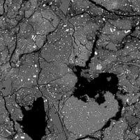
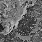
This is a scanning electron microscope image of gemstone processing waste. Researchers at Wuzhou University and Guangzhou University in China are exploring ways to use gemstone processing waste in cement, reducing the environmental impacts of both industries. Silicion carbide is an inert substance used as a grit in gemstone polishing. Using the polishing waste as an additive in cement helps to keep silicon carbide out of landfills. As a bonus, the waste has been found to enhance thermal conductivity by up to 159% and reduce electrical resistivity by up to 94% in the resulting cement. Courtesy of Xiaowei Ouyang.
November 2025

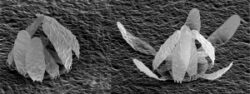
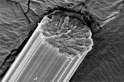
This image was the first-place winner in Class 4 (Artistic Microscopy–Color) of the 2025 International Metallographic Contest that was held in Detroit on October 19, 2025. The image is titled, “Penguin, Microstructure of Ti-6Al-4V Alloy Etched with Modified Weck’s Reagent, Mag.12.5x, Polarized Light, Light Microscopy.” Congratulations to the contributor, Lukasz Boron of the Łukasiewicz Research Network – Krakow Institute of Technology in Poland.
October 2025
This microstructure of anodized aluminum is viewed at 50X magnification. In order to perform materials characterization, certain color operations are needed to eliminate the internal dark divisions of grain as well as to highlight the grain boundaries. The grain size can be characterized by using polarized light via equipment such as the Clemex Vision system. Courtesy of Clemex.
September 2025
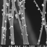
Using a transmission electron microscope (TEM) at the UC Irvine Materials Research Institute, researchers at the California Institute of Technology (Caltech) discovered that alloys produced using their hydrogel infusion-based additive manufacturing (HIAM) method form more homogenously, resulting in higher degrees of symmetry throughout their crystal structure. As shown in this micrograph, the final step in HIAM removes oxygen, leaving a mostly dense copper-nickel alloy in the desired, 3D-printed honeycomb structure. Courtesy of Thomas Tran at Caltech.
August 2025
This microstructure was taken of a spot weld in a high-strength, low-alloy steel (HSLA). It shows the solidification direction with the center of the weld nugget off the left of the image, near the center. This image of HSLA 350, captured using light optical microscopy using polarized light plus sensitive tint, was contributed by George F. Vander Voort, FASM.
This figure is among the growing collection of over 4400 micrograph images and associated data in the Micrograph Database published by ASM International, in cooperation with IMS.
July 2025
This secondary electron SEM image of iron film grown from Fe2O3 powder, is part of the research University of Oregon chemists conducted in an effort to discover a greener way to make iron metal for steel production. Paul Kempler and his team reported a way to create iron with electrochemistry, using a series of chemical reactions to turn saltwater and iron oxide into pure iron metal. They concluded that it’s the shape and porosity—not the size—of metal oxide particles that matter for efficiency in electrochemical ironmaking. Their method is a step toward cleaning up an industry that is one of the biggest contributors to carbon emissions worldwide. Courtesy of ACS Energy Letters, 2025.
June 2025
This image shows a steel sample deoxidized with aluminum in a vertical tube furnace at 1873 K. The sample was polished using grit papers ranging from P100 to P2500 and coated with platinum to reveal fine inclusions using focused ion beam-scanning electron microscopy (FIB-SEM). Interestingly, with the use of an optical microscope (ZEISS AXIO, 423730-9080), the image reveals bright, large spots resembling a typical supernova remnant in the Large Magellanic Cloud.
For context, a typical nebula such as the Cygnus Loop spans about 120 light-years—approximately 10²³ times larger than the bright spots observed in the image. The image was captured by Mir Ishfaq while he was a Ph.D. candidate and postdoc in the Department of Metallurgical Engineering and Materials Science at the Indian Institute of Technology (IIT) Bombay. Dr. Ishfaq is currently affiliated with the Department of Materials Science and Engineering at IIT Kanpur.
May 2025
This electron micrograph shows nanometer-thick kirigami structures that highlight the advantages of using rippled metamaterials as structural films. The alumina structures, resting on silicon wafers, are tested with lasers to measure behavior. The incorporation of rippled metamaterials allows for enhanced control over the final three-dimensional architecture and its mechanical properties. “This is the first time we can characterize precisely what the ripple effect is on thin film,” said Jian Zhou, assistant professor at the Thomas J. Watson College of Engineering and Applied Science’s Department of Mechanical Engineering. Zhou and his collaborators published a paper in the Proceedings of the National Academy of Sciences, 2025, doi.org/10.1073/pnas.2425200122. Image courtesy of Jian Zhou.
April 2025
A team from Northwestern University used scanning electron microscopy to create these images of fibers from engineered spider silk. Their research shows that the process of stretching spider silk aligns the protein chains within the fibers and increases the number of bonds, thus resulting in stronger tougher fibers. To validate their computational findings, the researchers used spectroscopy techniques to examine how the protein chains stretched and aligned in real fibers. Their work can be found in the paper “Charting the Envelope of Mechanical Properties of Synthetic Silk Fibers through Predictive Modeling of the Drawing Process,” Science Advances , 2025, doi.org/10.1126/sciadv.adr3833. Image courtesy of co-authors at Washington University at St. Louis.
March 2025
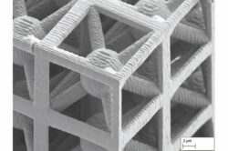
A new study from the Massachusetts Institute of Technology (MIT) presents a design framework for controlling ultrasound wave propagation in microscopic acoustic metamaterials. The researchers focused on cubic lattice with braces comprising a “braced-cubic” design. Through nondestructive, high-throughput laser-ultrasonics characterization, the team experimentally demonstrates tunable elastic-wave velocities within microscale materials. Their work paves the way for microscale devices and components that could be useful for ultrasound imaging or information transmission via ultrasound. Their paper, “Tailored Ultrasound Propagation in Microscale Metamaterials via Inertia Design,” was published in Science Advances, 2024, doi.org/10.1126/sciadv.adq6425. Courtesy of MIT.
February 2025
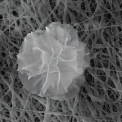
This elegant nanoflower adds antioxidant, antibacterial, and antibiofilm properties when applied to electrospun nanofiber bandages. For their bandage blooms, Fatemeh Ahmadpoor, Pier Francesco Ferrari, and their colleagues from the University of Genoa, chose copper(II) phosphate and tannic acid because of the antibiotic and anti-inflammatory properties of both reagents. After growing their flowers in a saline solution, the researchers attached the bioinspired structures onto strips of electrospun nanofiber fabric. Courtesy of ACS Applied Bio Materials, 2025, doi.org/10.1021/acsabm.4c00788.
January 2025
This image shows crush-lines in silicon nitride. It was among the top 20 entries in the Nikon Small World 1996 Photomicrography Competition. The image was captured at a magnification of 200x using darkfield microscopy. It was created by Ulbrich Buttner of Daimler Benz Research Center in Ulm, Germany.
December 2024
In a study by researchers at Griffiths’ Queensland Micro- and Nanotechnology Center, specific surface structures—called re-entrant microstructures—were studied for their ability to repel water and other liquids. Shown is an SEM image of a single re-entrant structure with a circular cap of SiO2. Scale bar: 5 µm. The study showed that re-entrant structures with larger gaps between them effectively trapped air pockets, enhancing water repellence and preventing the liquid from fully wetting the surface. These findings may open the way to developing materials that can withstand extreme conditions. Courtesy of Griffith University.
November 2024

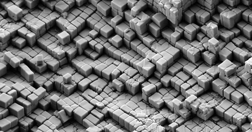
This image is a cross section of an iron nickel alloy that was made via powder bed fusion, giving it this unique tiled structure. The cross section was polished up to a 1um polishing pad and etched with Marble’s reagent to reveal the structure shown.
The image is courtesy of Matthew Roberts, associate metallurgist at Element Materials Technology in New Berlin, Wis.
October 2024
This image of graphene was captured using scanning tunneling microscopy. It is part of the research being conducted at Ames Laboratory at Iowa Statue University by Pat Thiel and Michael Tringides. They are investigating the unique properties of 2D materials and metals grown on graphene, graphite, and other carbon-coated surfaces.
“Graphene has gained a lot of enthusiastic attention in both scientific research and the tech industry because electrons travel very fast along its surface,” explained Tringides.
The team plans to write the rule book on the behavior of these materials. But their large goal is to create tunable materials that could be potentially useful in a host of tech applications, including ultrafast microelectronics, catalysis, and spintronics.
Courtesy of Ames Laboratory and the U.S. Department of Energy.
September 2024
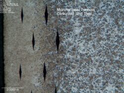
The micrograph of carburized 1215 steel shows the cause and effect of specific material processing. The increasing size of diamond-shaped indents, from left to right, indicates the increased hardness of the material. These defects were likely due to additional carbon diffusion into the metal. Courtesy of Metaltest Inc. and CES Engineering Guide.
August 2024
This image is of an electrolytic tin-plated steel surface. Viewed by episcopic illumination with crossed polarizers, the tin grains are easily visible. The center shows a large tin grain that’s a grayish color as opposed to the predominant blue. In an experiment, the stage was rotated 90°. The resulting image had the blue color in the center while all the surrounding area was gray. This color reversal is part of an optical staining technique used to highlight various features on the surface of the metals that are anisotropic-type materials. Courtesy of Wayne D. Niemeyer, “Ways to Examine Metals by Light Microscopy,” The McCrone Group.
July 2024
The butterfly-shaped image is an inclusion in low aluminum killed steel. An ingot was prepared by melting pure electrolytic iron and iron-aluminum alloy in an alumina crucible, followed by appropriate heat treatment. A sample was polished then ultrasonically cleaned with 99% reagent acetone. The inclusion was observed using a scanning electron microscope (Zeiss 45-58 Auriga Compact). Astonishingly, the right wing of the butterfly inclusion consists of pure Al2O3 inclusion, while the left one is composed of calcium oxide. The image was taken collaboratively by two Ph.D. students, Mir Ishfaq, and Sanjay Pindar, from Clean Steel Lab in the Department of Metallurgical Engineering and Materials Science at the Indian Institute of Technology Bombay, Mumbai.
June 2024

A metal alloy composed of niobium, tantalum, titanium, and hafnium has awed materials scientists with its impressive strength and toughness at both extremely hot and cold temperatures, a combination of properties that seemed so far to be nearly impossible to achieve. The image shows a map of the crystal structure of the remarkable alloy made with electron backscatter diffraction in a scanning electron microscope. Each color represents a section of the crystal where the repeating structure changes its 3D orientation. The alloy’s surprising properties were discovered by a team led by Robert Ritchie, FASM, at Lawrence Berkeley National Laboratory (Berkeley Lab) and U.C. Berkeley, in collaboration with the groups led by professors Diran Apelian, FASM, at U.C. Irvine and Enrique, FASM, at Texas A&M University. Their research was published on April 11, 2024, in Science. The alloy’s resilience to bending and fracture across an enormous range of conditions could open the door for a novel class of materials for next-generation engines that can operate at higher efficiencies. Courtesy of Berkeley Lab.
May 2024
This image of cartridge brass was from a failed rivet on a bulldozer. It shows compressed grain on the left from a cold heading operation. The larger grain on the right side is the stock wire. The micrograph, captured at 100x, was from a team project during Eisenman Materials Camp in 2000. The team was charged with investigating the failure of the brass rivet. After conducting various materials tests, the team concluded that the hardness specification for the brass rivet did not allow it to be ductile enough to pass the roll-over test. Suggestions to prevent this type of failure in the future were to lower the hardness specifications so the rivet could pass the roll-over test, or use steel as an alternative material. Courtesy of Michael B. Connelly and the Frog Consultants of Eisenman Materials Camp 2000.
April 2024
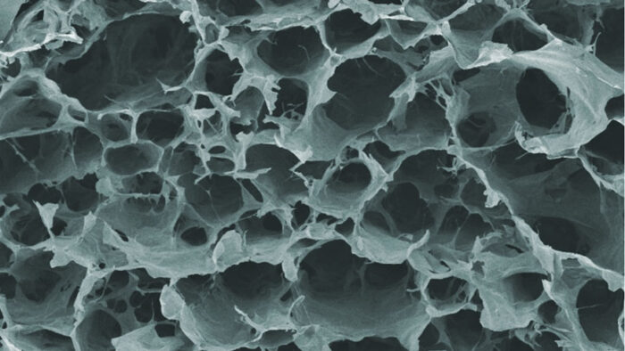
This airy structure of aerogel was imaged via electron microscopy and colored by researchers from Empa’s Cellulose and Wood Materials laboratory. The aerogel was a byproduct of the new process developed by Gustav Nyström’s team to produce high-quality nanocellulose from brewery waste. The spent grain that the researchers used for their experiments came from the Pentabier brewery in Dübendorf. They extracted the nanocellulose fibers from the grain and processed them into an aerogel by freeze-drying. This airy material contains a large number of pores, which gives it excellent thermal insulation properties. The versatile biodegradable raw material then can be made into packing materials or fiber-reinforced polymers. Courtesy of Empa.
March 2024
This scanning electron microscope image is of tin crystals, stimulated by electricity and growing on a copper surface. A new method developed by Princeton researchers could speed up the process of designing and testing new crystalline materials. Although computer simulations are commonly used in crystal design, the new method relies on a large language model, similar to those that power text generators like ChatGPT. Their research is published in the article “LLM-Prop: Predicting Physical and Electronic Properties of Crystalline Solids from their Text Descriptions.”Courtesy of Lynn Trahey/Argonne National Laboratory.
February 2024
This is a photo micrograph of lunar sample # 10022 gathered in 1969. The light blue and white mineral is plagioclase. The black is ilmenite, and the blue and/or green and/or orange and/or yellow and/or red mineral is pyroxene. The large pyroxene is a phenocryst that had been partially resorbed. Magnification one inch equals one-tenth millimeter. This is one of the many lunar samples collected by astronauts Neil A. Armstrong and Edwin E. Aldrin Jr. during the Apollo 11 lunar landing mission. The many samples they collected have been subjected to extensive tests and examinations at the Manned Spacecraft Center’s Lunar Receiving Laboratory. Courtesy of NASA.
January 2024
This image is an optical micrograph showing the chiral liquid crystal phase of a polymer that researchers at the University of Illinois Urbana-Champaign are exploring to produce highly efficient semiconductor materials. By making small tweaks to the structure of the non-chiral polymer called DPP-T4, they could alter the torsion or the twist of the structure and induce chirality. Chirality is one of nature’s strategies used to build complexity into structures, with the DNA double helix as the most recognizable example. Using x-ray scattering and imagining, the team found that their “slight tweaks” caused major changes in the phases of the material. The changes in the complex mesophase structures that were formed may lead to optical, electronic, and mechanical properties unimagined before. Courtesy of Ying Diao Lab.
December 2023
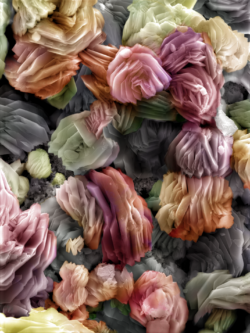
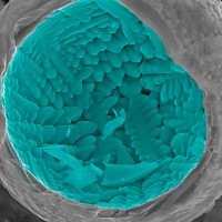
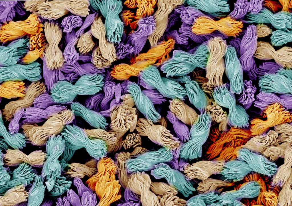
This image is the winner of Class 4 (Artistic Microscopy – Color) in the 2023 International Metallographic Contest. The contest was held during the International Materials, Applications & Technologies Conference and Exhibition in Detroit in October. This winning entry, called, “Crystal Bouquet,” was submitted by Michelle Chambers of Eurofins | EAG Laboratories. The image was captured on a Tescan Mira SEM at a magnification of 3130x. The image was colored in Photoshop.
November 2023
ASM and IMS are embracing the spooky this time of year. While it might look like a spider in its web, this image is an excellent example of a sand cast, white cast iron with 4.3% C. Viewed after etching with 4% picral acid, flake graphite in a region of hypereutectic white iron is revealed in this light optical micrograph. Original image by Leonard Samuels.
October 2023
This image is of a 431 stainless steel, etched with modified Murakami’s. The image was captured at a magnification of 400X via digital image correlation. Courtesy of Pace Technologies. Visit the website at metallographic.com.
September 2023
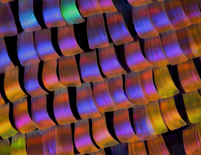
This image captures wing scales of the twilight moth Urania ripheus. The image was achieved using a focus stacking technique, in which many photos are taken at different depths and then stacked using software. The image won Honorable Mention in the Olympus/Evident Image of the Year Award 2020 contest. Courtesy of Walter Ferrari of Argentina.
August 2023
This Hollow Sphere of FeO won first place in the Artistic Microscopy (Color) class during the 2022 IMS International Metallographic Contest held during IMAT in New Orleans last September. The image shows the alloys’ dendritic structure as well as its hollow nature. It was captured by Demmys Kelsen Florentino de Sousa from the Center for Gas Technology and Renewable Energy (CTGAS-ER – Centro de Tecnologias do Gás e Energias Renováveis) in Brazil.
July 2023
Materials researchers at the University of Kiel, Germany, have recently developed a novel soft, conductive material that can be used in robotic applications. Unlike conventional soft conductors, it shows remarkably stable electrical properties even upon deformation. The material is made of fine wires. The wires consist of interconnected microtubes made of an electrically conductive polymer. Under the scanning electron microscope, the basic structure of the material looks like a porous sponge, that can be easily compressed. Nanoscale coatings can be applied to provide additional properties Courtesy of the University of Kiel, Germany.
June 2023
This scanning electron microscope image, captured at high magnification, shows fatigue striations in a steel bolt. The bolt displayed significant beach marks, indicating that the crack growth occurred over some period of time.
The image can be found in ASM Handbook, Volume 11: Failure Analysis and Prevention in the article “Microfractography and Metallography for Failure Analysis” by Frauke Hogue, FASM.
May 2023
Micron-scale bow ties with candy-wrapper twists are shown in this colorized electron microscope image. The ability to control the degree of twist in a curling, nanostructured material could be a useful new tool in chemistry and machine vision. The bowties are made by mixing cadmium metal and cystine, a protein fragment that comes in left- and right-handed versions, in water spiked with lye. If the cystine was all left-handed, left-handed bow ties formed. Likewise, right-handed cystine yielded right-handed bow ties. A team from the University of Michigan produced 5000 different shapes within the bow tie spectrum. They studied the shapes in atomic details using x-rays at Argonne National Laboratory before conducting simulation analysis. Courtesy of Prashant Kumar, Kotov Lab, University of Michigan.
April 2023
This image shows fracture surface of the equimolar HfMoNbTiZr refractory high entropy alloy having BCC crystal structure. The fracture surface was examined by using a tabletop scanning electron microscope (Hitachi TM1000) and the image was captured under back-scattered electron mode at the magnification of 2500X. The image is presenting characteristic features of brittle fracture (cleavage fracture) evidenced by river lines within a single grain. This image was used for the study of the mechanical properties, failure analysis, and surface modification of engineered materials. Courtesy of the Mechanical Metallurgy Research Group of İstanbul Technical University.
March 2023
This microscopy-generated image shows the path of a fracture and accompanying crystal structure deformation in a CrCoNi alloy at nanometer scale during stress testing at 20 Kelvin (-424 F). The fracture is propagating from left to right. The image was part of a study on high-entropy alloys conducted by researchers from Berkeley Lab and Oak Ridge National Lab. The team measured the highest toughness ever recorded of any material when studying this chromium, cobalt, and nickel alloy. Courtesy of Robert Ritchie/Berkeley Lab.
January 2023
This image shows fracture surface of the equimolar HfMoNbTiZr refractory high entropy alloy having BCC crystal structure. The fracture surface was examined by using a tabletop scanning electron microscope (Hitachi TM1000) and the image was captured under back-scattered electron mode at the magnification of 5000X. The image is presenting characteristic features of brittle fracture (cleavage fracture) evidenced by the presence of river lines within the grains. This image was used for the study of the mechanical properties, failure analysis, and surface modification of engineered materials. Courtesy of the Mechanical Metallurgy Research Group of İstanbul Technical University.
December 2022
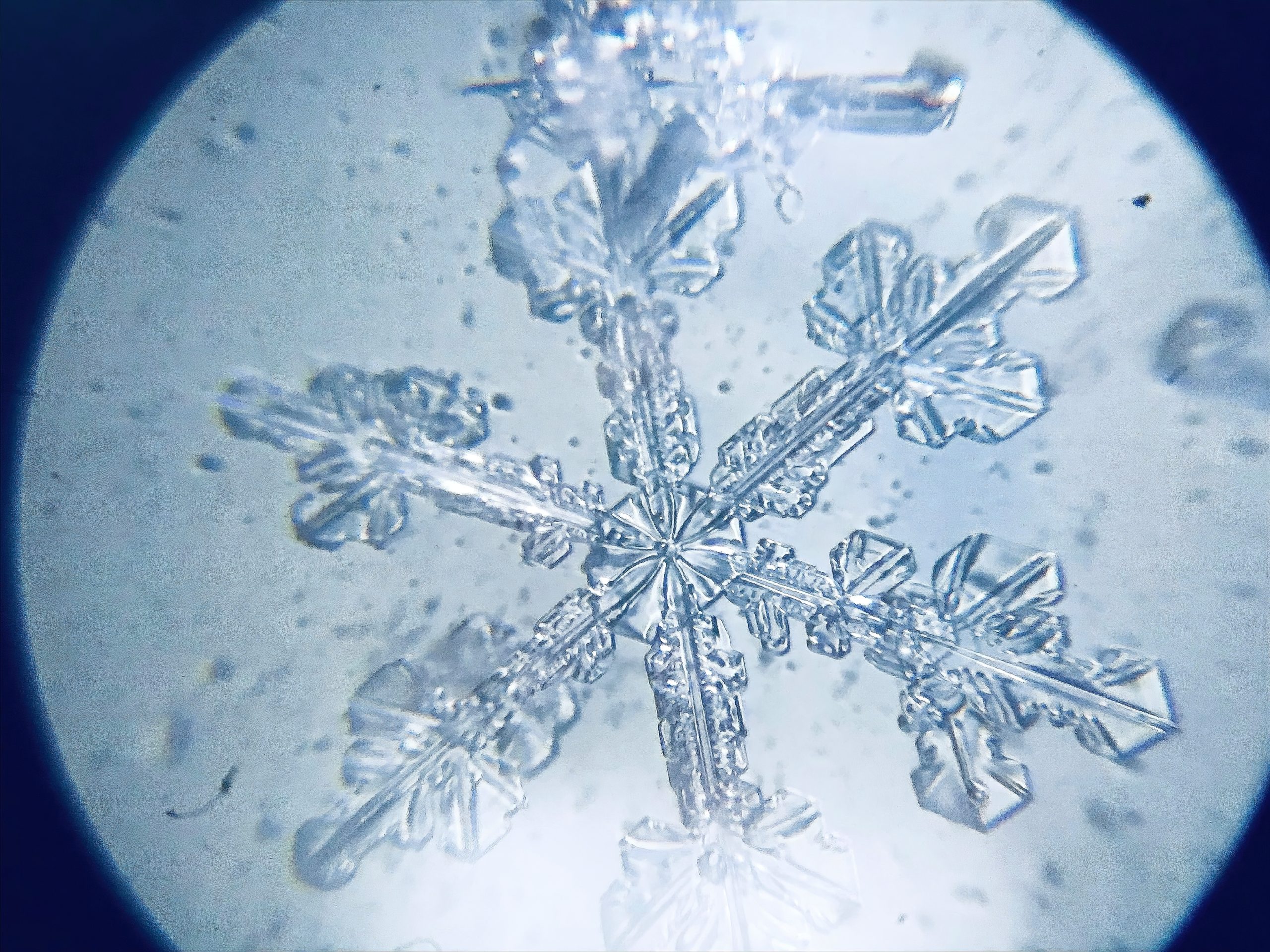
This wintry image is of a snowflake ice crystal stellar dendrite under a microscope. Stellar dendrites typically have six main branches that are all relatively symmetrical. Courtesy of Dreamstime.com.
November 2022
This image shows iron powder combusted in an industrial-scale burner, used for the application of sustainable energy carrier. It was part of a recent study by scientists from the Max-Planck-Institut für Eisenforschung (MPIE) and the Eindhoven University of Technology. They were examining how to store and transport excess energy efficiently. For example, in peak times of wind and sun, excess energy is produced that is needed in times of less wind and sunshine. The researchers analyzed how metals, particularly iron, can be used for energy storage and which parameters determine the efficiency of the storage and reuse. Their sustainability study showed that using metals to store energy is feasible. Future studies will analyze how to increase the circularity of the process, as the size of some combusted particles is decreased compared to their original size due to partial iron evaporation, micro-explosions and/or fracture of some iron oxide particles. They published their recent findings in the journal Acta Materialia (“Phase transformations and microstructure evolution during combustion of iron powder” ). Courtesy of Laurine Choisez, Max-Planck-Institut für Eisenforschung.
October 2022
This captivating micrograph by Sheri Neva of EAG Eurofins Los Angeles, received first place in Class 5 Artistic Microscopy (Black & White) in the 2022 International Metallographic Contest. The event was held in New Orleans during the International Materials Applications & Technologies Conference and Exhibition. The Moth Fly, aka Dragon Fly, was coated with 6Å of iridium using the Quorum Q150T coater. The image was taken using a Tescan Mira field emission scanning electron microscope. A secondary electron image was captured at 150x magnification. Ms. Neva, a member of the ASM Los Angeles Chapter and the Failure Analysis Society, initially found the subject flying around her office.
September 2022
This micrograph was created by high school students at the Eisenman Materials Camp at ASM International in Materials Park, Ohio, in July. The group was charged with studying the failure of a lawnmower blade, which exhibited a highly corroded fracture surface. The end of the blade showed heavy wear and abrasion. The sample was first cleaned using Alconox and analyzed using a Zeiss scanning electron microscope. The part was also optically analyzed at 1000x longitudinally at the fracture surface. A series of micrographs showed evidence of corrosion over time as well as abnormal cracks. The group concluded that the part was manufactured inexpensively, then overused and overstressed in service, and subjected to loading and unloading at the brittle fracture site, which ultimately led to the break. Courtesy of Anna Kuan, Alla Fuener, John Morton, Jackie Lin, Daniel Lamping, and Jude Narayana guided by mentors Allie Glover, Tom Glasgow, and Kendall McCord.
August 2022
A zoomed-in image of the structure of one of the pieces of meteorite from an asteroid named Ryugu, captured by the spacecraft Hayabusa2, which landed in Australia in 2020. The petrography of the rock fragment—Ryugu sample C0002-C1001—resulted in this backscattered electron (BSE) image, which shows brecciated matrix. The black spaces in the figure are pores. The texture is similar to CI chondrites, a group of rare stony meteorites belonging to the carbonaceous chondrites. Courtesy of JAXA/Yokoyama et al.
July 2022
Petrographic thin section of iron ore under the microscope and with polarized light. Thin sections are geological samples for microscopy. The rock is an iron ore from the Banded Iron formation of Precambrian age from Australia. The brown parts represent the iron.
June 2022
This scanning electron microscope image is a single laser scan cross-section of a nickel and zinc alloy. The image was taken as part of quest to create defect-free metal parts laser powder bed fusion. Here dark nickel-rich phases interleave lighter phases with uniform microstructure. A pore can also be observed in the melt pool structure. Courtesy of Raiyan Seede, Texas A&M. Research collaborators include Ibrahim Karaman, FASM; Raymundo Arroyavé, FASM; and Alaa Elwany. For more information, see the researchers’ findings in the journal Additive Manufacturing.
May 2022
This micrograph is of an 1851 historical copper coin from Chile. The image shows corrosion at the edge and detail of slight porosity. The reagent used during sample preparation was an alcoholic solution of 2% ferric chloride (FeCl3). Magnification 100×. Courtesy of Patricia Silvana Carrizo.
For more information, see the article “Archaeometallurgical Study of Two Ancient Copper Coins” in Advanced Materials & Processes magazine, April 2022.
April 2022
This image is the catastrophic result of passing too much charge through a nanoscale electrical contact. The huge amount of heat generated has blown a hole in the gold contact pad, melting the metal that has solidified as droplets in this “splash effect” revealing the silicon dioxide and pure silicon substrate underneath. The scanning electron micrograph was taken on a Zeiss Supra Scanning Electron Microscope. Courtesy of the Advanced Microscopy Lab at Trinity College Dublin.
March 2022
This image, which won the Grand Prize in the 2021 EIPBN Micrograph Contest, is of sodium chloride crystals captured on an electrospun composite air filter. It was captured on a Hitachi S4500 Field Emission SEM. Courtesy of EIPBN Micrograph Contest (Zyvex Labs), Luke J. Suttey, Sowmya Sudhakar, Jessica M. Andriolo, and Jack L. Skinner of the Montana Tech Nanotechnology Laboratory at Montana Technological University in Butte. The contest is part of the International Conference on Electron, Ion, and Photon Beam Technology and Nanofabrication.
February 2022
The image is of as-cast wrought-grade aluminum alloy (Al-Mg-Fe-Si containing < 1wt.% of each solute) with no addition of grain refinement particles. This micrograph illustrates one of the possible growth morphologies that a solidifying metal can adopt. The dendritic structure is the result of instabilities in the solid-liquid interface during growth due to the rejection of solute into the liquid phase. Dendritic grains are more prevalent in alloys of high solute content and larger grain sizes. The Barker’s etch and applied electrical field produce a thick oxide layer on the grains of aluminum (anodizing). When viewed in cross-polarized light, interference in the oxide layer produces colors, which depend on grain orientation and oxide thickness; hence the grain structure is imaged. Courtesy of T. Quested, Department of Materials Science and Metallurgy, University of Cambridge.
January 2022
This image shows an etched cross-sectioning beneath tensile fracture surfaces (necking) of carbon steel at 500x through the Nomarski. Elongated grains toward the fracture are visible. The image was tested, prepared, and captured by Ehsan Ahi at Velan Metallurgical Laboratory, Montreal, Canada.
December 2021
This SEM micrograph details a fast fracture overload area of a fractured Nitinol wire-form component. Microvoid coalescence is observed on the fracture surface in this area. The image is from the article “Fatigue Fracture of Nitinol” by which appeared in the October 2021 issue of SMST NewWire. Courtesy of Louis G. Malito et al. from Exponent Inc. Click here to learn more
November 2021
This pocket of dendrites was found when sectioning through an experimental nickel superalloy casting. The image was captured using a TESCAN VEGA3 in secondary electron mode (ETD). The specimen was rotated and tilted to capture both the cut surface as well as dendrites in the cavity. Aside from contrast/brightness adjustments within the SEM software, no digital processing was used to enhance the image. The image was created by Adam Haskins of Forensic Metallurgy in Phoenix. It was submitted to the IMS International Metallographic Contest held during IMAT 2021 and won First Place in the Artistic Microscopy – Black and White class.
October 2021
The image was created by annealing C26000 brass at 800°C for two hours to create very large grains, then a Leco AMH55 automated microhardness tester was programmed to create the columbine flower pattern. The sample was then annealed to cause localized recrystallization and controlled grain growth at 525°C in the areas of high dislocation density. Next, the sample was polished to remove the indentations, and etched with Klemm’s II etchant using DIC illumination on an Olympus DSX500. This image was submitted by W. Preston Cole, Robert S. Crow IV, Grace A. Rome, Carmen M. Sanchez, Gregory D. Vigil, Addison C. Wong, and Gerald R. Bourne to the IMS International Metallographic Contest held during IMAT 2021.
September 2021
This image captures a single crystal of tetracene, grown on an indium-tin-oxide coated glass slide using a vapor-liquid-solid deposition technique. A grid pattern of SU-8 photoresist pillars was created on the glass slide prior to crystal growth. It was submitted by Griffin Reed of Western Washington University / Midwestern University to the 2021 JEOL Image Contest in the SEM category. Reed captured the image with a field emission scanning electron microscope (JEOL JSM-7200F).
August 2021
The morphology of bitumen surfaces has been identified in the past by atomic force microscopy and scanning electron microscopy. But what still remained a mystery was whether its surface and chemical compositions correlate with each other. Now materials chemists Dr. Ayse Koyun and Prof. Hinrich Grothe from TU Wien, Vienna, have examined the bitumen surface using various physicochemical analysis methods and learned more about how to decelerate the oxidation process thus, slowing the aging of the material.
July 2021
This striking image was created by Amir Ardalan Rezaie and Reza Abbashian, FASM, University of California, Riverside. It earned the First-Place award in Class 4—Artistic Microscopy (Color) at the 2018 International Metallographic Contest. Titled “Deeply Etched Graphite Yellowstone,” the image graces the cover of Guenter Petzow’s Metallographic Etching, 2nd Edition, published by ASM International.
June 2021
This image is part of the 2020 Jacquet-Lucas Award winning entry in the International Metallographic Contest. Submitted by Lavinia Tonelli of the University of Bologna, Italy, it was part of her study on metal powders for additive manufacturing. The image is of a Co28Cr6Mo alloy for a biomedical application processed by laser power bed fusion. It was captured with high magnification light microscopy with polarized light. To learn more about how these powders were investigated and characterized, click here to read the article “Using Conventional Light Microscopy to Reveal the Hierarchical Microstructure of 3D-Printed Metal Parts” in the May/June issue of Advanced Materials & Processes magazine.
May 2021

This image shows the microstructure of nickel/chromium rich boride in the athermally solidified zone (ASZ). The BNi2 brazing alloy is shown at 1000 x. The image was prepared and captured by Ehsan Ahi laboratory supervisor and metallurgist, Velan Inc., Montreal, Canada.
April 2021
An entry in the SEM category of the 2021 JEOL Image Contest, this “cocoon” depicts thermally treated tin oxide. It was submitted by Alexandre de Oliveira Jorgetto. The image was captured with a field emission scanning electron microscope (JEOL JSM-7500F).
March 2021
In this image, courtesy of the CMU Holm Group, a computer vision (CV) system finds powder particles in an SEM micrograph of a metal powder used in additive manufacturing (AM). The CV system can detect individual particles, even when they overlap. To learn more about how these powder particle masks are used in novel characterization methods to identify satellite particles that can affect the flowability of AM powders, read the article “Computer Vision and Machine Learning to Quantify Microstructure” in the February/March issue of Advanced Materials & Processes magazine. Click here to read the full article.
February 2021
This scanning electron microscope image of lithium titanate (lithium, titanium, oxygen) nanoflowers had a unique origin. On the frontier of energy storage, scientists at Brookhaven National Laboratory gained useful insights into materials for making better batteries. These included discovering how structural defects can improve performance and developing a way to increase capacity of a promising high-rate electrode material featuring this unique flower-shaped nanostructure. Varying the concentration of chlorine, lithium, and reaction time, allowed the highly crystalline nanoflowers to bloom.
January 2021
To create the subject of this image, 60 nm of gold was deposited on a heat shrinkable polymer. The film was heated at 200°C for 3 minutes to form a nano-folded gold catalyst for the electroreduction of CO2. It was captured with a JEOL JSM-IT100 SEM. The image was the February 2020 selection in JEOL’s SEM/TEM/EPMA Image Contest. Image courtesy of Kam Sang Kowk of Johns Hopkins University, Baltimore.
December 2020
This image of cuboidal Ni3Al precipitates (edge length ~400 nm) in a Ni-based single-crystal superalloy won first place in the 2019 Royal Microscopical Society’s Scientific Imaging Competition. These precipitates are the source of the outstanding strength of superalloys at high temperatures, enable the operation of turbine blades in the extreme environments within jet engines. The sample provided by BIAM was etched to reveal the precipitates. Courtesy of Alessandro Piglione.
November 2020
This colorized SEM micrograph by Amir Farkoosh, a postdoctoral researcher in the Materials Science and Engineering Department at Northwestern University, Evanston, Ill., received first place in Class 4 Artistic Microscopy (Color) in the 2020 International Metallographic Contest. The micrograph displays the as-solidified dendritic microstructure of a dilute aluminum-hafnium solid-solution alloy. The sample was ground with a series of SiC papers and then electropolished utilizing a solution of 10% nitric acid in ethanol at -10°C. The backscattered electron image was acquired utilizing an FEI Quanta 650 field emission gun SEM.
October 2020
This image reveals the contrasting microstructural constituents of different materials. The ferrite in the steel is colored, while the iron carbide is kept white to achieve a clear contrast of the carbide precipitations. The color etching technique used resulted in the formation of sulphate layers of different thicknesses on the grain or mixed crystal areas. Sections were etched in Klemm or Beraha. Both are tint etchants based on potassium sulphite. The composition was provided in Metallographisches, keramographisches, plastographisches Ätzen by Günter Petzow and Veronika Carle, published in 2006 by Borntraeger. Courtesy of Leica Microsystems.
September 2020
This SEM image shows exfoliated vermiculite, which is a hydrated magnesium-aluminum-iron silicate. The majority of applications call for vermiculite in its exfoliated form, created when the flakes are heated rapidly at a temperature of 900°C or higher. The water flashes into steam, and the flakes expand into accordion-like particles. The image was a previous grand prize winner in Thermo Fisher Scientific’s Image Contest. Courtesy of Francisco Rangel, National Institute of Technology-INT/MCTI, Brazil.
August 2020
This micrograph by Sheri Neva of EAG Eurofins Los Angeles, received first place in Class 5 Artistic Microscopy (Black & White) in the 2019 International Metallographic Contest. The subject is a Spiky Caterpillar found outside Southern California, which was gold coated and imaged in JEOL6610LV at 300x. The imaging technique used was a mix of 60% SEI and 40% BEC.
July 2020
This microstructure shows the hydrogen induced cracking in the acicular ferrite of high-strength low-alloy (HSLA) steel subjected to aging treatment. The image presents the nucleation of crack through in the niobium carbide. The sample was etched with a Nital (2% nitric acid in ethanol) reagent to reveal steel microstructure. The micrograph was captured at a magnification of 2000x using a scanning electron microscope. Courtesy of terminal project of M.S. Alberto López Leyva in Metallurgical Engineering at Universidad Autónoma Metropolitana-Unidad Azcapotzalco, Ciudad de México.
June 2020
This electron backscattered diffraction image was obtained by the Tescan scanning electron microscope at the University Instrumentation Center, University of New Hampshire (UNH). It shows the microstructure of a hot-rolled WE43 magnesium alloy used in rotary parts due to its light weight, high strength to weight ratio, and nice cyclic behavior. The current image is an inverse pole figure map, and the recrystallized grains are located in a line along with the rolling direction. The sample preparation included grinding with SiC grinding papers followed by polishing with diamond paste. An etchant of 60 vol.% ethanol, 20 vol.% distilled water, 15 vol.% acetic acid, and 5 vol.% of nitric acid for about 5 seconds was applied. Courtesy of Saeede Ghorbanpour, Marko Knezevic’s lab, Mechanical Engineering Department, UNH.
May 2020
This image shows the microstructure of Norem hardfacing. It was etched by picric acid + hydrochloric acid + ethanol solution and captured at a magnification of 1000× with use of interference-contrast illumination (DIC microscopy). Courtesy of Ehsan Ahi, laboratory supervisor and metallurgist, Velan Inc., Welding and Metallurgical Center of Excellence, Montreal, Canada.
April 2020
Lamellas were ion-milled in fluorescent polysterene spheres to create this award-winning image. Captured using a ThermoFisher Hellos Ux-G4, the image received an Honorable Mention award in the 2019 EIPBN Micrograph Contest. The contest is held annually during the EIPBN Conference, an international meeting dedicated to lithographic science and technology and its application to micro and nanofabrication techniques. Courtesy of Sergey Gorelick of Monash University, Australia.
March 2020
This stacked microscopic photo shows cuprite, which is a mineral composed of copper oxide (Cu2O). It was captured with a 20× objective lens. The image ranked in the top 20 out of more than 2,000 entries in the 2019 Nikon Small World Photomicrography Competition. Courtesy of Dr. Emilio Carabajal Márquez, Madrid, Spain.
February 2020
This microstructure is an electron backscatter diffraction (EBSD) map acquired from the Tawallah Valley meteorite, Australia. It is a ferrite inverse pole figure with respect to the horizontal direction. The map shows that there are multiple orientations present. The image can be found in the newly revised ASM Handbook, Volume 10: Materials Characterization, in the article “Crystallographic Analysis by Electron Backscatter Diffraction in the Scanning Electron Microscope” by Joseph R. Michael, Sandia National Laboratories. Volume 10 provides detailed technical information that will enable readers to select and use analytical techniques that are appropriate for their problem.
January 2020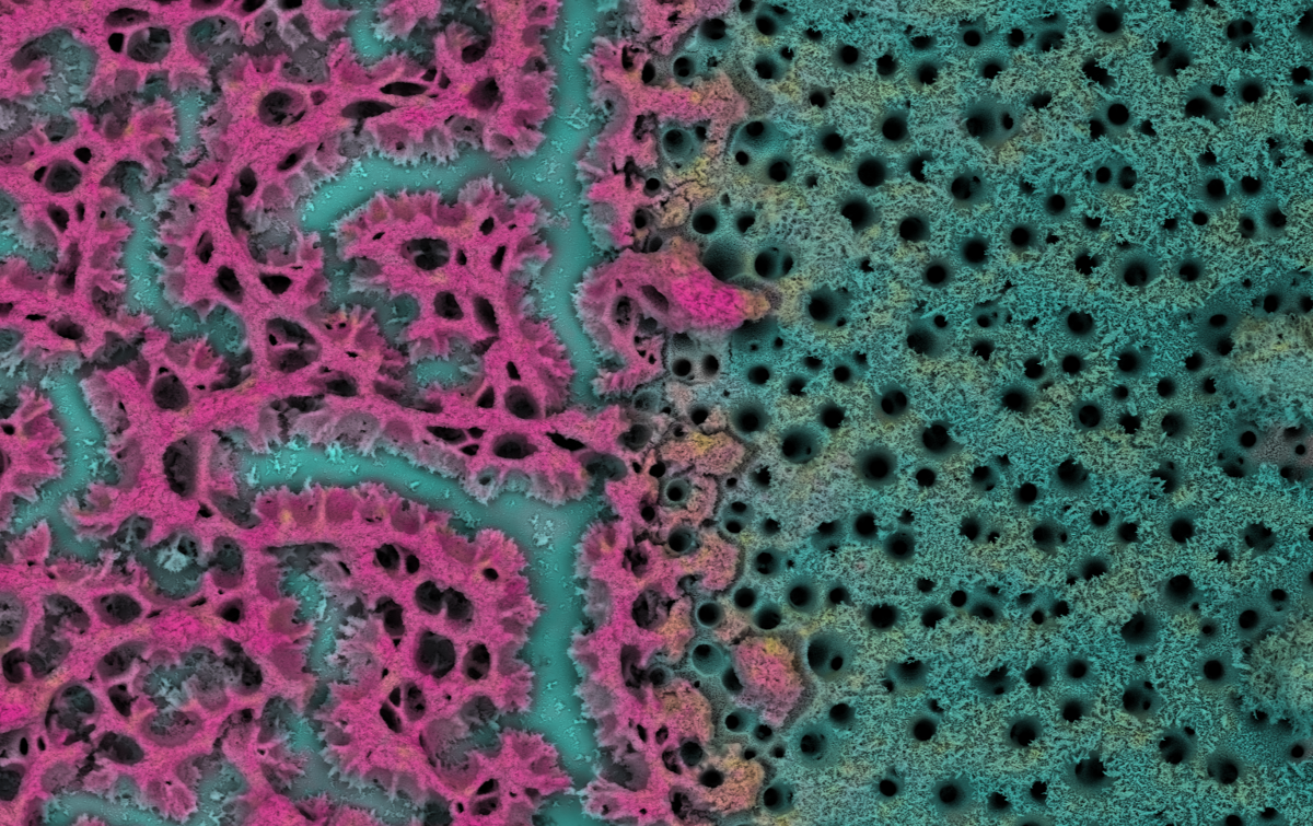
This image is electroplated bimetallic metal foams can be used as catalysts for the electrochemical reduction of CO2 into carbon monoxide and alcohols. This color SEM image is courtesy of Dr. Peter Broekmann, Department of Chemistry and Biochemistry, University of Bern, Switzerland. Read more about the benefits of color imaging in the Thermo Fisher article “Next-Gen Color Technology Changes How Materials Are Characterized,” in the January issue of Advanced Materials & Processes magazine.
December 2019
This image is a magnified view of a meteorite specimen from Mars under cross-polarized light. The image was taken with the University of Delaware’s (UD) new atomic force-Raman microscope. The meteorite was among samples that came to the team from NASA’s Johnson Space Center and from the Smithsonian. A UD research team headed by Dr. Karl Booksh will be studying the chemical composition and properties of the rocks. Their work could aid the search for life on Mars in NASA’s and the European Space Agency’s 2020 rover missions. Courtesy of University of Delaware.
November 2019
This image “Dawn to Dusk” was submitted by Sam Luther of The Ohio State University. This image received first place in Class 4 Artistic Microscopy (Color) of the 2019 International Metallographic Contest. The background is a 10,000×-magnification image of the fracture surface of ductility-dip cracking in a nickel-based filler metal 52M multipass weld. Thermal faceting was observed on the surface, the varying topography of which serves as the background for each individual color. The high resolution and high depth of field were achieved on an FEI Sirion SEM at OSU’s Center for Electron Microscopy and Analysis.
October 2019
 This image “Blue Lagoon” shows the microstructure of the fusion zone between Stellite alloy 6 hardfacing (polished condition) and F91 base metal. It was etched by picric acid + hydrochloric acid + ethanol solution and captured at a magnification of 1000× with use of interference-contrast illumination (DIC microscopy). Courtesy of Ehsan Ahi, laboratory supervisor and metallurgist, Velan Inc., Welding and Metallurgical Center of Excellence, Montreal, Canada.
September 2019
![]()
This electron backscatter diffraction (EBSD) image of beta processed Ti6246 titanium was submitted by ASM President David Furrer, FASM. The sample was polished through conventional methods and vibratory final polished prior to alpha grain orientation imaging. EBSD image courtesy of Greg Levan and David Furrer (Pratt & Whitney).
August 2019
The image “Scanned Snickers Treat” is when Students attending the 20th Eisenman Camp at ASM Headquarters in July toured the Parker Hannifin Computed Tomography Lab, where they were treated to multiple images of a Snickers bar. Shown is a one-plane image of a 3D volume of the bar. The sweet was analyzed with a Nikon XT H 225 CT scanner, taking roughly 6000 2D x-ray images at various angles. The details appeared after the images were reconstructed to a 3D volume. Materials Camp mentors used the candy to illustrate fractures, by pointing out the cracks in the chocolate and peanuts.
July 2019
This image “I See a Green Future” by Emmanuel V. Péan, shows a perovskite layer magnified 10 times using an optical microscope. Perovskite materials are good candidates for inexpensive solar panels. The image won a Runner-up Award in the 2018 Research as Art competition conducted by Swansea University in Wales.
June 2019
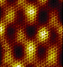
This image “Waves of Grain” shows the interference of electron waves on the surface of a material, as measured with a scanning tunneling microscope. The waves form when electrons scatter off surface defects, which are visible as brighter features in the image. The waves are part of “The world’s most stable microscope” story featured in this issue. Courtesy of Leiben University/Irene Battisti.
May 2019
This image “Winning Stir Weld” was part of the 2017 Jacquet-Lucas winning submission by Elvin Beach of Worthington Industries Inc. and Thomas Luzanski, Dustin Marshall, and Brain Dix of TWB Co. LLC. The micrograph depicts friction stir welded AA 6022 (left) and AA 5182 (right) sheets of different thicknesses, magnification 50x. Etching reveals a clear oxide line at the weld interface and additional oxide lines in alloy 5182 near the weld root and in alloy 6022 near the weld face (far right side).
April 2019
“Metallic Wood”, In a new study published in Nature Scientific Reports, university researchers announce that they have fabricated a sheet of nickel with nanoscale pores that make it as strong as titanium but four to five times lighter. The image shown is a microscopic sample of the researchers’ “metallic wood.” Its porous structure is responsible for its high strength-to-weight ratio, and makes it more akin to natural materials, like wood. The scientists are from the University of Pennsylvania’s School of Engineering and Applied Science, the University of Illinois at Urbana-Champaign, and the University of Chicago.
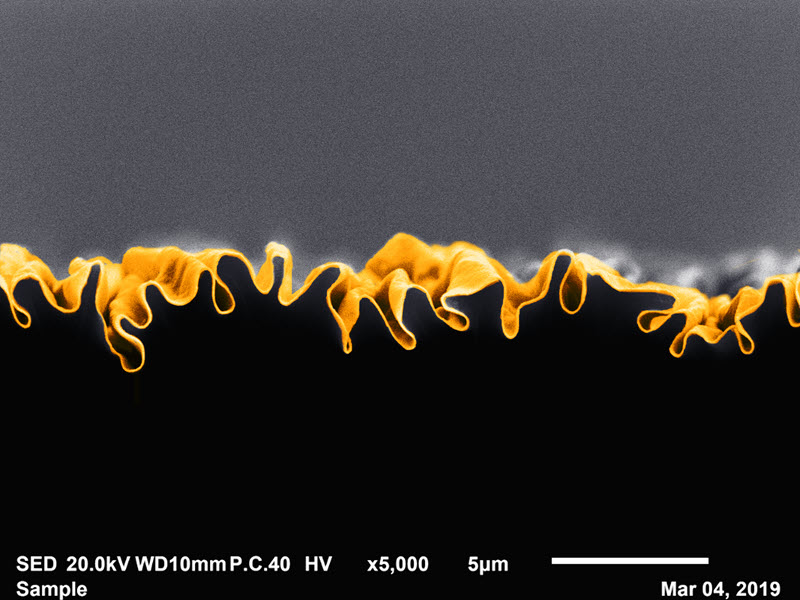
March 2019
This image “Petal to the Metal” is a bullet made of 0.95% antimonial lead with copper plating. The copper plating had a severe defect—a porous band. The sample was etched with an ammonium molybdate/nitric acid reagent. The image was captured at 50× with dark field illumination and shows a petal partially torn off from penetration into ballistic gelatin. The petal and the region near it were severely deformed and the lead recrystallized to small grains as compared with the lead microstructure in the interior, which was a result of age hardening. Courtesy of Stephen Gladieux, Lewiston, Idaho.
February 2019
This image ” Copper Kaleidoscope” is a copper grid (front) with its demagnified and distorted reflection in a concave electron mirror. A Zeiss SEM was used at 1000× by Navid Abedzadeh of MIT, Cambridge, Mass., to capture the artistic shot. The image was selected as the Best Electron Micrograph during the 61st International Conference on Electron, Ion and Photon Beam Technology and Nanofabrication (EIPBN). The image competition is aptly named the EIPBN Bizarre/Beautiful Micrograph Contest.