Detecting ‘hidden defects’ that degrade semiconductor performance with 1,000X higher sensitivity
January 15, 2026 Source: ASM International
Semiconductors are used in devices such as memory chips and solar cells, and invisible defects that interfere with electrical flow may exist within them. A joint research team at the Korea Advanced Institute of Science and Technology (KAIST) and IBM T. J. Watson Research Center has developed a new analysis method that can detect these “hidden defects” (electronic traps) with approximately 1,000 times higher sensitivity than existing techniques.
The technology is expected to improve semiconductor performance and lifetime, while significantly reducing development time and costs by enabling precise identification of defect sources.
The research team developed a new measurement technique that can simultaneously analyze defects that hinder electrical transport (electronic traps) and charge carrier transport properties inside semiconductors. They published their results in Science Advances.
Within semiconductors, electronic traps can exist that capture electrons and hinder their movement. When electrons are trapped, the electrical current cannot flow smoothly, leading to leakage currents and degraded device performance. Therefore, accurately evaluating semiconductor performance requires determining how many electronic traps are present and how strongly they capture electrons.
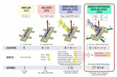
The research team focused on Hall measurements, a technique that has long been used in semiconductor analysis. Hall measurements analyze electron motion using electric and magnetic fields.
By adding controlled light illumination and temperature variation to this method, the team succeeded in extracting information that was difficult to obtain using conventional approaches.
Under weak illumination, newly generated electrons are first captured by electronic traps. As the light intensity is gradually increased, the traps become filled, and subsequently generated electrons begin to move freely. By analyzing this transition process, the researchers were able to precisely calculate the density and characteristics of electronic traps.
The greatest advantage of this method is that multiple types of information can be obtained simultaneously from a single measurement. It allows not only the evaluation of how fast electrons move, how long they survive, and how far they travel, but also the properties of traps that interfere with electron transport.
The team first validated the accuracy of the technique using silicon semiconductors and then applied it to perovskites, which are attracting attention as next-generation solar cell materials.
As a result, they successfully detected extremely small quantities of electronic traps that were difficult to identify using existing methods—demonstrating a sensitivity approximately 1,000 times higher than that of conventional techniques.
Professor Byungha Shin stated, “This study presents a new method that enables simultaneous analysis of electrical transport and the factors that hinder it within semiconductors using a single measurement,” adding that “it will serve as an important tool for improving the performance and reliability of various semiconductor devices, including memory semiconductors and solar cells.”
Image – Conceptual diagram of the evolution of hall characterization (analysis) techniques. Credit: Science Advances (2026).
For more information:
The Korea Advanced Institute of Science and Technology
https://www.kaist.ac.kr/en/
Subject Classifications
Electronics
Electronics and Microelectronics
Failure Analysis
materials characterization
Nanotechnology
news
News Articles


